

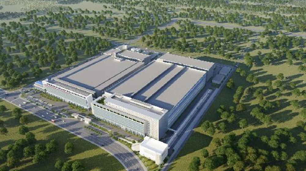
The Hefei Comprehensive Bonded Zone Electronic Information Standardized Plant Project is part of the development of Crystal Union Integrated Circuit. As the first 12-inch foundry enterprise in Anhui Province and the third-largest pure wafer foundry enterprise in China, it has achieved mass production from 150nm to 90nm process nodes and is currently undergoing customer product verification for 55nm. The launch of the third phase of the project will help Crystal Union Integrated Circuit successfully complete the IPO process. With a construction area of approximately 420,000 square meters and a planned total investment exceeding 100 billion yuan, the project aims to achieve a total capacity of 320,000 wafers per month. The construction scope includes the installation, commissioning, and power supply of FAB buildings, CUP buildings, medium-voltage cabinets, low-voltage cabinets, and transformer equipment within the substation.


 网站首页
网站首页