

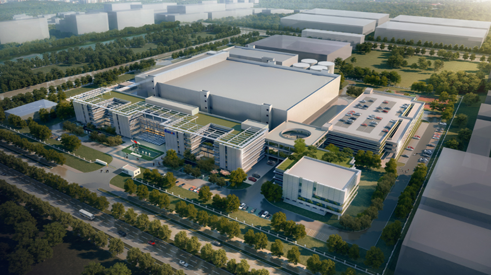
The Shanghai Geke Semiconductor 12-inch CIS Integrated Circuit Feature Process R&D and Industrialization Project is the first large-scale integrated circuit wafer manufacturing project to settle in the Lingang New Area after its establishment. It lays a solid industrial foundation for the construction of the Oriental Silicon Harbor characteristic park and helps improve the integrated circuit industry ecosystem in the Lingang New Area. It will also drive industrial agglomeration and promote industrial scale enhancement in the new area. Once completed, it will have the capability to produce 720,000 wafers annually with independent intellectual property rights, integrating from IC design to chip manufacturing as an IDM-type company. The construction scope includes public cable tray systems, strong and weak electrical systems, lighting systems, clean ventilation and air conditioning systems, water supply and drainage systems, process cooling water systems, vacuum systems, compressed air systems, and general electromechanical systems.


 网站首页
网站首页